# GCD Design Based on Modelsim (Verilog)
这是课程 <工程创新设计 Ⅳ> 的课程设计,我基于 verilog 语言设计了一个 GCD 模块
# Abstract
This project is based on the design concept of a state machine and employs the algorithmic idea of successive subtraction. It uses the Verilog language to describe the circuit and designs a set of circuits capable of efficiently and accurately calculating the greatest common divisor (GCD). The project includes calculations of the circuit's timing and uses the Monte Carlo method to estimate the average clock cycles. Comprehensive simulation tests have been conducted, including multiple sets of correct input data as well as several sets of unexpected input tests.
Keywords: Verilog, Successive Subtraction, Greatest Common Divisor (GCD), Monte Carlo Method
# I. Design Purpose
This experiment aims to implement a circuit using Verilog language that can calculate the greatest common divisor (GCD) of two 32-bit unsigned numbers within a certain period of time.
# II. Design Idea
# 1. The idea of the GCD algorithm
The calculation of the greatest common divisor (GCD) is usually accomplished using the method of successive subtraction or successive division. Since the successive division method involves division operations, it will occupy more resources in the circuit. In this design, we implement the GCD calculation using the successive subtraction method.
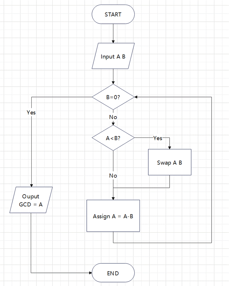
The algorithm implementation of calculating the GCD using successive subtraction is shown in Figure 1.

Figure 1 Block Diagram of the Successive Subtraction Algorithm
First, the two operands, A and B, are read in. A loop is then executed, with the exit condition being B = 0. Within the loop, the value of A and B is first compared. If A is less than B, A and B are swapped. Then, A - B is calculated and the result is used as the new value of A. When the loop ends, the value of A is the greatest common divisor of the inputs.
We assume that neither of the input numbers A and B is zero, and both are 32-bit unsigned integers. If one of the numbers is zero, the output will be the value of the other number. The Verilog description will also follow this convention.
# 2. Signal List Definition
The definitions of input and output signals are shown in Table 1 below.
| Signal | IO | Width | Description |
|---|---|---|---|
| clk | IN | 1 | Input clk signal, 1MHz |
| rst | IN | 1 | Asynchronous reset signal, active high |
| a_in | IN | 32 | Operand A for GCD calculation |
| b_in | IN | 32 | Operand B for GCD calculation |
| run | IN | 1 | Start signal for calculation, active high, maintained for one clock cycle |
| done | OUT | 1 | Calculation completion signal, active high, maintained for one clock cycle |
| gcd | OUT | 32 | Result of the calculation |
Table 1 IO Signal List
The definitions of internal signals are shown in Table 2 below.
| Signal | Width | Description |
|---|---|---|
| a | 32 | Operand A during the calculation process, initially latched from a_in |
| b | 32 | Operand B during the calculation process, initially latched from b_in |
| minus | 32 | The difference between operands A and B, continuously assigned |
| state | 2 | Current state |
| next_state | 2 | Next state |
Table 2 Internal Signal List
# 3. State Machine Design
From the algorithm description of the greatest common divisor (GCD) calculation, we find that the process of calculating the GCD mainly involves two types of operations: comparison and swapping, and calculating the difference. Therefore, in this design, four states: IDLE (Idle state), SWAP (Swap operands state), SUB (Subtraction operation state), and DONE (Calculation completion state), are defined. The meanings and functions of these four states are shown in Table 3 below:
| State | Meaning | Description |
|---|---|---|
| IDLE | Circuit IDLE | Indicates that no calculation is currently being performed. The circuit will automatically return to the IDLE state when it is reset or after completing a round of calculation. |
| SWAP | Swap Operands | The circuit compares the value of the two operands and decides whether to swap them based on the comparison result. |
| SUB | Substraction Operation | The relative sizes of the operands have already been ensured. The larger operand is subtracted by the smaller one, and the result is latched. |
| DONE | Calculation Done | Indicates that the calculation of GCD is complete. It is important to note that the DONE state will only be maintained for one clock cycle. After one clock cycle, the state will automatically switch back to IDLE. |
Table 3 State Description
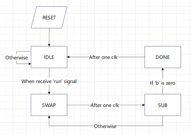
The transitions between the four states are shown in figure 2.

Figure 2 State Transition Diagram
When the circuit is reset, it automatically enters the IDLE state.
In the IDLE state, the circuit waits for the run signal. If the run signal is valid, the next state transitions to SWAP; otherwise, it remains in the IDLE state.
In the SWAP state, the next state automatically transitions to the SUB state.
In the SUB state, if the b signal is 0, the next state transitions to DONE, indicating that the calculation is complete; otherwise, the next state transitions back to SWAP, indicating that the successive subtraction operation continues.
In the DONE state, the next state automatically transitions back to the IDLE state.
# III. Implementation Details and Partial Code
# 1. Definition of Variables and States
Define 32-bit internal variables a, b, and minus. Since a and b are assigned values within an always block, they are defined as reg type. Since minus is continuously assigned and represents the difference between a and b, it is defined as wire type. Additionally, use localparam to define the four states, and define state and next_state as 2-bit wide reg type variables.
1 | reg [31:0] a; |
# 2. Implementation of the State Machine
In the implementation of the state machine, we adopt a three-segment approach:
For the state transition part, sequential logic is used:
1 | always@(posedge clk or posedge rst) begin |
On each rising edge of the clock, the state is updated to the next state. A high-level asynchronous reset is used, which resets the state to IDLE.
The calculation of the next state is implemented using combinational logic:
1 | always@(*) begin |
First, next_state is assigned the value of the current state to avoid latches.
Then, based on the value of state and the state transition logic described earlier, the value of next_state is updated according to the conditions.
The latching of operands, swapping of operands, subtraction of operands, and the final result output are implemented using sequential dlogic:
1 | always@(posedge clk or posedge rst) begin |
On reset, the internal variables a and b, as well as the output signals gcd and done, are non-blocking assigned to 0.
In the IDLE state, the values of a_in and b_in are continuously sampled and latched into a and b, and the values of gcd and done are non-blocking assigned to 0.
In the SWAP state, if a < b, non-blocking assignment is used to swap the values of a and b.
In the SUB state, the value of minus is non-blocking assigned to a.
In the DONE state, the value of a is non-blocking assigned to gcd to indicate the output result, and the value of done is non-blocking assigned to 1 to indicate a valid output.
# IV. Timing Calculation
# 1. Estimation of Clock Cycles for GCD Calculation
Let the number of iterations for successive subtraction be N (one iteration is defined as the comparison and subtraction operations). In my design, both the SWAP state and the SUB state consume only one clock cycle each. Therefore, the estimated time for one GCD calculation can be expressed as 2N+2, where 2N represents the SWAP and SUB states, and the additional 2 accounts for the IDLE and DONE states.
# 2. Worst-Case Clock Cycle Scenario
The worst-case scenario occurs when and . In this case, A is reduced by B in each iteration, requiring rounds of successive subtraction. The clock cycle consumption reaches the order of . This level of time consumption is unacceptable. The following solutions can be considered:
Special Case Handling
Special-case handling for B=1 can be implemented, but this is only a temporary fix. It is still possible to construct data that consumes a large number of clock cycles, and special-case handling complicates the circuit.
Implementing Division
Division can be implemented by following the approach humans use for division, starting with the most significant bit to determine the highest bit of the result, and then proceeding to the lower bits. This method can significantly improve the timing performance, achieving a logarithmic time complexity O(logn), where the number of operations depends on the number of bits. However, implementing division is complex, and it is not considered in this design. The following section will show that a good timing performance can be achieved on average.
# 3. Estimating Average Clock Cycles Using the Monte Carlo Method
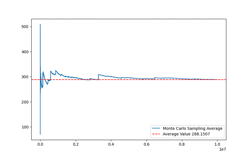
The Monte Carlo method involves using a large number of simulation experiments to estimate the average value of a quantity. In this case, I wrote a Python script to randomly generate two 32-bit unsigned integers and calculate the number of rounds of successive subtraction required to complete the GCD calculation. By generating multiple sets of random numbers and taking the average, an estimate of the average clock cycle consumption can be obtained. The Python script is included in the appendix. The experimental results are shown in the figure below.

Figure 3 Estimation of Average Clock Cycles Using the Monte Carlo Method
After conducting experiments with 107 sets of random numbers, it was found that the average number of iterations stabilizes around 288. This means that the average clock cycle consumption is approximately 578. This performance is acceptable for random data, which is why the successive subtraction method is used.
# V. Simulation
In the testbench, multiple sets of data were used for testing. To ensure the completion of the calculation, an interval of 300 or 600 clock cycles was introduced between each round of input. The testbench code is detailed in the appendix.
# 1. Simulation Testing with Arbitrary Input Numbers
Three sets of data were tested here: (88, 156), (26400, 46800), and (15015, 12345). The numbers in the parentheses represent the inputs a and b, respectively.
# Data Set 1(88,156)
The waveform is shown in Figure 4.

Figure 4 Simulation Waveform for (88, 156)
The meanings of the signals are referred to in the previous sections, and the current state is displayed by state_name. It can be seen that the final calculated result gcd = 4 is correct.
# Data Set 2(26400,46800)
The waveform is shown in Figure 5.

Figure 5 Simulation Waveform for (26400, 46800)
It can be seen that the final calculated result gcd = 1200 is correct.
# Data Set 3(15015,12345)
The waveform is shown in Figure 6.

Figure 6 Simulation Waveform for (15015, 12345)
It can be seen that the final calculated result gcd = 15 is correct.
These three sets of data initially verify the correctness of the circuit in calculating the greatest common divisor (GCD).
# 2. Testing with Erroneous Data
# Simulation Test with One Input as Zero
The input data is (0, 4), and the waveform is shown in Figure 7.

Figure 7 Simulation Waveform for (0, 4)
It can be seen that within one round of successive subtraction operations, the circuit detected that one of the operands was 0 and thus output the other operand as the result.
# Simulation Test with Both Inputs as Zero
The input data is (0, 0), and the waveform is shown in Figure 8.

Figure 8 Simulation Waveform for (0, 0)
It can be seen that the circuit correctly provided the result.
# 3. Continuous Input Testing
For the sake of design simplicity, this design does not specifically address the continuous input scenario. It is assumed that new inputs are accepted only after the completion of the calculation. To verify the robustness, the non-normal condition of continuous input was tested here. Two sets of data, (26400, 46800) and (88, 156), were input with intervals shorter than the calculation time, and the waveform is shown in Figure 9.

Figure 9 Simulation Waveform for Continuous Input
It can be observed that when the second set of data was input continuously, the circuit did not sample the new input but continued with the original calculation and eventually output the correct result for the first set of data.
When faced with continuous input, the circuit prioritizes completing the original calculation instead of recalculating based on the new input. This design approach is reasonable.
# VI. Summary
Summary
During the course, I had a relatively smooth experience with Verilog syntax since I had previously learned some basics. This allowed me to keep up with the course content quite quickly. However, the teacher's explanations provided me with a deeper understanding in several areas. For example, I learned more about the implementation of FPGAs using lookup tables, the structure of circuits with sequential logic intermixed with combinational logic, and the differences between non-blocking and blocking assignments. I gained a more profound understanding in many aspects.
Problem
The main issues I encountered were related to software usage and some code details. For instance, while writing the testbench file, I accidentally named the test module the same as the module itself. This caused the simulation to fail to produce any results. I resolved this issue by seeking help from the teacher. At that time, I lacked experience in this area and couldn't identify the error. After the teacher pointed it out, I became more mindful of module naming conventions. Now, I can quickly address similar issues if they arise in the future.
# VII. Appendix
# 1. gcd.v
1 | module gcd( |
# 2. tb_gcd.v
1 |
|
# 3. MonteCarlo.py
1 | ''' |